


Silicon Carbide wafer SiC crystal substrate wafer
Negotiable Min Order Quantity Unit
- Required Quantity
-
- Place of Origin
- China
- Payment Terms
- T/T
- Production method
- Negotiable
- Shipping / Lead Time
- Negotiable / Negotiable
- Category
- Semiconductors
![]()
Suzhou Hengmairui Materials Technology Co.,Ltd.
 China
China
- Verified Certificate
-
10


| Product name | Silicon Carbide wafer SiC crystal substrate wafer | Certification | - |
|---|---|---|---|
| Category | Semiconductors | Ingredients | - |
| Keyword | sic crystal substrate wafer , silicon carbide wafer , sic substrate | Unit Size | - |
| Brand name | - | Unit Weigh | - |
| origin | China | Stock | - |
| Supply type | - | HS code | - |
Product Information
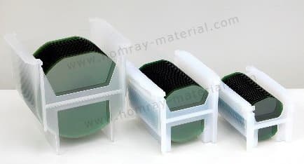
Homray Material Technology provide high quality silicon carbide wafer to electronic and optoelectronic industry. Silicon carbide wafer is a next generation semiconductor material, with unique electrical propertiesand excellent thermal properties , compared to silicon wafer and gallium arsenide wafer , silicon carbide wafer is more suitable for high temperature and high power device. Silicon carbide wafer can be supplied in diameter 2 inch,3 inch,4inch,6inch , both 4-H-N or 6-H-N or 4/6H-Si.
Homray Material Technology offers silicon carbide wafers in different grades.
Standard quality wafers meet high demands for production purposes, research grade substrates are the inexpensive alternative for research and development and for process trials.
B2B Trade
| Price (FOB) | Negotiable | transportation | - |
|---|---|---|---|
| MOQ | Negotiable | Leadtime | Negotiable |
| Payment Options | T/T | Shipping time | Negotiable |
![]()
- President
- Cory
- Address
- LiSheng Industrial Building,60 Suli Road
- Product Category
- Semiconductors
- Year Established
- 2009
- No. of Total Employees
- 51-100
- Company introduction
-
Homray Material Technology(HMT)was established in 2009, is a leading manufacturer and supplier of Gallium Nitride(GaN) Substrate Wafer(GaN-On-Sapphire Template, Free-standing GaN Wafer), GaN Epi Wafer (GaN-On-Si Epi Wafer, GaN-On-Sapphire Epi Wafer, GaN-On-SiC Epi Wafer), and Silicon Carbide(SiC) Substrate Wafer, SiC Epi Wafer, Silicon Test Wafer etc. It is widely acknowledged that compound Semiconductor (GaN, SiC) with its superior property like wide-bandgap, is expected to the most promising material choice for next generation device. GaN device/module and SiC device/module can achieve low losses and fast switching/oscillation simultaneously because of its high critical electrical field. Homray Material Technology is committed to developing high quality GaN Wafer and SiC Wafer for HEMT RF, power electronics and opto-electronics applications. As the leading Substrate Wafer and Epi Wafer manufacturer and supplier in the semiconductor industry, our dealers and partners are mainly distributed in Europe, USA, Southeast Asia, and South America, our sales value exceeded 65 Million US dollars in 2020. Excellent products quality and professional service won the trust and support from our customers in the world as well as our share of market.
- Main Product


Related Products

12 WAFER CASSETTE (ELECTROLESS NICKEL PLATING

Hi-Fix Board

On-Device Edge AI

Silicone Rubber Products

DDR RAM, SSD, Flash, Memory Card
