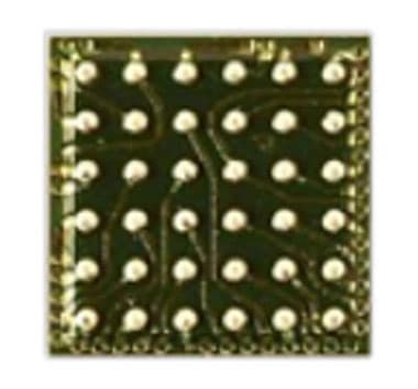
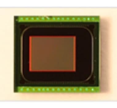
Wafer-Level Packang (WLP)
Negotiable Min Order Quantity Unit
- Required Quantity
-
- Place of Origin
- Brand name
- SARAM
- Payment Terms
- Negotiable
- Production method
- Negotiable
- Shipping / Lead Time
- Negotiable / Negotiable
- Keyword
- camera module, science, semiconductor, semiconductor chip
- Category
- Semiconductors
SARMA International
- Country / Year Established
-
 South Korea
/
- Business type
- Others
- Verified Certificate
-
11


| Product name | Wafer-Level Packang (WLP) | Certification | - |
|---|---|---|---|
| Category | Semiconductors | Ingredients | - |
| Keyword | camera module , science , semiconductor , semiconductor chip | Unit Size | - |
| Brand name | SARAM | Unit Weigh | - |
| origin | Stock | - | |
| Supply type | - | HS code | - |
Product Information
Wafer-Level Packang (WLP)
This new Solution is based Tessera's industry-proven SHELLCASE wafer-level chip scale packaging (WLCSP) tech nology, which provides the benefits of reduced cost and accelerated time-to-market, without the need for modification or redesign to the image sensor wafer.
OEM and camera module manufacturers need to meet market demand for smaller profile, thinner and more sophisticated mobile devices. The SHELLCASE MVP solution provides the answer, offering image sensor packaging solutions that are thinner, more reliable and at a lower cost. The end result is higher device functionality and increased board capacity, which enables the next generation of smaller, smarter and faster electronics devices.
This new solution is based on Tessera’s industry-proven SHELLCASE wafer-level chip scale packaging (WLCSP) technology, which provides the benefits of reduced costs and accelerated time-to-market, without the need for modification or redesign to the image sensor wafer.
The innovative SHELLCASE MVP solution utilizes an encapsulated, glass-silicon sandwich structure to enable image-sensing capabilities through the actual packaging structure. Encapsulation of chip and interconnects provides a break-through in true WLCSP solutions.
The SHELLCASE MVP solution is offered in both cavity and non-cavity formats and leaded or lead-free bump formats. And the flexible package design and structure enable the incorporation of filters, as well as use of different package materials or processes, providing additional advantages for manufacturers.
>>FEATURES
- No modification or redesign of image sensor wafer.
- Extremely cost-effective package.
- Electrophoretic encapsulation of the package for automotive applications.
- Contact possible with standard metal pads.
- Applicable for all scribe line widths.
- Optical properties are characterized by glass cover with transmittance of 91.2% for cavity and 95.2% for non-cavity in 350nm-900nm range.
- Extremely accurate die rotation control during assembly (max. <+ 0.01°)
- Precise die tilt control of <0.5mil during assembly.
- Reduced SI thickness to meet small pitches.
- Termination type: BGA or LGA
B2B Trade
| Price (FOB) | Negotiable | transportation | - |
|---|---|---|---|
| MOQ | Negotiable | Leadtime | Negotiable |
| Payment Options | Negotiable | Shipping time | Negotiable |
- President
- June, Yoo
- Address
- B-dong 206, Works Building Garden 5, Munjung-dong, Songpa-gu, Seoul, Korea
- Product Category
- Other Machinery & Industry Equipment,Semiconductors
- Company introduction
-
Welcome ! Welcome to our e-catalog home. Here you can find information about our products. You can also send us inquiries and post comments about our company and products. We hope you enjoy your visit.
- Main Product
Related Products
Sputtering targets (metal, alloy, oxide, ceramic targets and others)
_2.jpg)
MFC (Mass Flow Controller)
Hafnium oxide, HfO2, sputtering target, evaporation material, thin film coating material
EMI Shielding Metal Spring Gasket
12 WAFER CASSETTE (ELECTROLESS NICKEL PLATING


