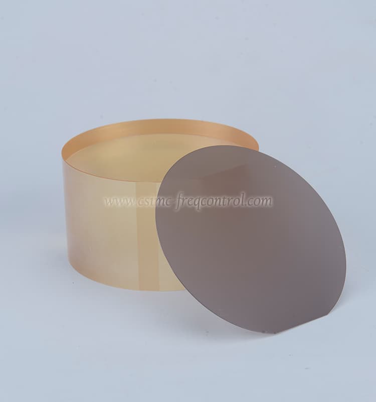
Fe doped LT Wafers
Negotiable Min Order Quantity Unit
- Required Quantity
-
- Place of Origin
- China
- Payment Terms
- Negotiable
- Production method
- Negotiable
- Shipping / Lead Time
- Negotiable / Negotiable
- Keyword
- lithium tantanlate wafer
- Category
- Quartz Products
Hangzhou Freqcontrol Electronic Technology Ltd.
- Verified Certificate
-
7

| Product name | Fe doped LT Wafers | Certification | - |
|---|---|---|---|
| Category | Quartz Products | Ingredients | - |
| Keyword | lithium tantanlate wafer | Unit Size | - |
| Brand name | - | Unit Weigh | - |
| origin | China | Stock | - |
| Supply type | - | HS code | - |
Product Information
B2B Trade
| Price (FOB) | Negotiable | transportation | - |
|---|---|---|---|
| MOQ | Negotiable | Leadtime | Negotiable |
| Payment Options | Negotiable | Shipping time | Negotiable |
- President
- Tianhua Wu
- Address
- NO.1106, Crystal International Business Center(CIBC), No.198 Wuxing Rd ,Qianjiang new city, Jianggan district, Hangzhou, P.R.China
- Product Category
- Quartz Products
- Year Established
- 2000
- No. of Total Employees
- 101-500
- Company introduction
-
Splitting up from former China National Scientific instrument and materials company in 1999 , Hangzhou Freqcontrol Electronic Technology Ltd. is a leading Chinese manufacturer who involves in piezoelectric crystals , surface acoustic wave filters and the single crystal growth as well as substrates process which for use in the telecommunications and general time and frequency industries.
Rely on our manufacturing facilities and our sister partners we register this organization as CQT (China Quartz Technology ) for the strategic cooperation, we are able to supply a very broad range of all high precision single quartz blanks with all different possible orientation for TC control ; lithium Niobate and lithium Tantalate substrates (3”,4” and 6” ) for RF signal picking up in Smart Mobile and all Custom sized special glass substrates for Optical windows as well as all commercial-end frequency controlled component at BULK and SAW industry for 3G,4G,and 5G application. Optical Grade Quartz Wafers, Fe doped LT Wafers, Finsihed Crystal Manufacturer .
We has been servicing for microelectronic manufacturers, defense related contractors, National laboratories, universities and scientists around the world since 1990 . our expertise is specialty on the single piezo crystal science , all kinds of quartz blank and lithium Niobate Lithium Tantalate wafer manufacture, We are committed to the supply of all types of substrate wafers to the microelectronics industry.
We focus on innovation, cost-effectiveness, and superior quality for our customers. Our accomplishments are the result of the combined efforts of all of our employees, who are dedicated to the highest ethical and quality standards.From 2007 marked our continued expansion with the addition of LN ,LT ,QTZ substrate products on 3” , 4” and also 6” with the most thinner at 0.1-0.15 mm which will make chips to be possible to be packed within more the most of smallest packages.
Up to 2010 years, we developed production capability to all different kind of glass substrates up to 12” to apply for both semiconductor and optical industry.Expansion into existing markets with leading edge products that exploit today's advanced manufacturing technologies has become the mainstay of our successful business growth.
- Main Product
Related Products
Vietnam Quartz Countertops
China Quartz Stone,Engineered Marble,Artificial Stone Supplier
Natural Silica Sand
Quartz Heater Chemical Vapor Deposition
Copper Copper Alloy Tubes and Pipes


 China
China


